

Best Semiconductor Equipment Connectors for Cleanroom Performance and Reliability
2026-11-17
In semiconductor manufacturing, even the smallest connector failure can compromise cleanroom integrity and bring production to a halt. This guide examines what separates high-performance equipment connectors from ordinary components, highlighting how REUNION addresses the demands of ultra-clean environments with reliable, contamination-resistant solutions.
Surface Finish Details That Control Particle Release Around Wafer Handling
Surface finish around wafer handling is rarely just about roughness averages. The features that matter are the sharp micro-peaks left by machining, the shallow pull-out pits from media blasting, and the way a grain boundary opens into a fine crevice after passivation. Particles tend to lodge in those recesses during cleaning and later release when a load, rotation, or small misalignment flexes the component. A slightly textured surface can actually hold fewer large particles than a visually bright finish if the peaks are rounded and the valleys are open enough to drain.
The more consistent predictor is the quality of edge and transition areas. Holes, chamfers, recesses, and weld seams often carry burrs or smeared metal that ordinary area roughness measurements ignore. Under wafer contact or pneumatic actuation, these features act like tiny scrapers, generating particles long after the main surface has been polished. For that reason, specifying finish across the full part including thread roots, vent slots, and the backside of a pocket matters more than chasing a low Ra on the primary face.
Electropolishing helps only when the underlying machining damage has been removed first. If deep tool marks remain, the process dissolves the peaks and leaves narrow, high-aspect-ratio valleys that can trap slurry residues. A better approach is to define the finish by particle release testing after a realistic cleaning cycle, rather than by a single profile number. That shifts attention from appearance to how the surface behaves through repeated handling, purge, and contact with the wafer edge.
Contact Geometry and Signal Stability in Vacuum Chamber Tooling
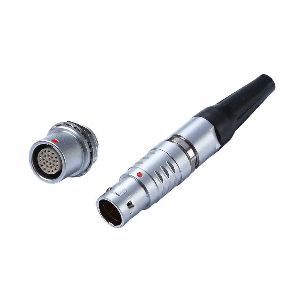
The way a probe or clamp seats against a wafer carrier inside a vacuum chamber rarely gets the attention it deserves. Small mismatches in contact geometry, such as a slightly tilted pad or an edge that lifts by a few microns, produce intermittent resistance changes that look like signal drift. Once the chamber is pumped down, thermal contraction and outgassing can exaggerate those micro-gaps, turning a bench-level pass into an unstable in-situ measurement.
A useful approach is to map the actual footprint instead of relying on the nominal surface profile. Pressing a sacrificial carbon film or using a low-current continuity scan across the tooling interface reveals where the true load path sits. When the contact patch is centered and sufficiently broad, the return path stays quiet even as chamber pressure cycles. By contrast, a narrow line contact concentrates current density and makes the signal vulnerable to local oxidation or vibration.
Stability improves when the tooling is designed to float slightly during the initial pump-down and then lock once thermal equilibrium is reached. This lets the mating surfaces settle into a repeatable position rather than fighting the chamber's deflection. It also helps to reduce the number of stacked interfaces between the sensor, the carrier, and the feedthrough, since each additional boundary adds a potential discontinuity.
Material Pairings That Lower Outgassing Without Sacrificing Conductivity
Silver-coated copper wire paired with nickel barrier layers has become a practical choice in vacuum relays and sealed switchgear. The nickel film, typically 2–5 microns thick, blocks copper migration and reduces volatile organic residues that would otherwise condense on nearby optics or insulators. Conductivity stays within a few percent of bare copper at DC and low-frequency AC, while outgassing rates measured by ASTM E595 drop below 0.1% TML and 0.01% CVCM, which is often clean enough for high-voltage aerospace harnesses.
Gold over palladium on beryllium-copper springs offers a different balance. Palladium acts as a diffusion stop, preventing the underlying beryllium and copper from reaching the gold surface and forming resistive oxides or carbon-rich films during bake-out. In cryogenic slip rings and thermal vacuum chambers, this stack keeps contact resistance under 10 milliohms after 1,000 mating cycles while keeping collected volatile condensable material under 0.05%. The gold top layer handles the actual current path, so the slight resistivity penalty of palladium never shows up in the contact interface.
For PCB-level grounding in ultra-high-vacuum instruments, tin-silver-copper solder joints with a conformal parylene mask outperform bare HASL or ENIG finishes. The parylene adds a 2-micron barrier that suppresses outgassing from flux residues and epoxy substrates, yet the tin-silver-copper alloy maintains a bulk conductivity around 12% of copper and a joint resistance below 1 milliohm per via. Thermal desorption spectra from these boards show most species desorbing below 150°C, leaving only trace water vapor above 200°C—clean enough for mass spectrometers and electron beam columns.
Sealing and Shielding for Wet Benches, Gas Panels, and Robotic Cells
Wet benches, gas panels, and robotic cells each bring their own set of contamination and safety demands, yet they share a common weak point: the gaps where enclosures meet service penetrations, viewports, and cable drops. A practical sealing strategy starts by treating those interfaces not as afterthoughts but as part of the airflow and pressure design. For wet benches, that often means pairing chemical-resistant gaskets with drip-edge profiles that direct stray liquids away from electrical compartments. Gas panels require a different mindset—here the priority shifts to maintaining low leak rates under thermal cycling, so stainless steel spring-energized seals or graphite-filled options frequently replace softer elastomers that can cold-flow or degrade in the presence of process gases.
Shielding adds a second layer that goes beyond simple containment. In robotic cells, for instance, the motion of articulated arms can create transient pressure differentials, pulling unfiltered air into supposedly clean zones. Rather than relying on a single continuous bead of sealant, a more robust approach combines labyrinth-style mechanical barriers with low-outgassing polymer strips that flex without losing contact. On gas panels, electromagnetic and radio-frequency shielding often needs to coexist with gas-tight sealing; this can be achieved by specifying conductive elastomer gaskets that carry a fluoropolymer coating, preserving chemical compatibility while still grounding stray currents across flange faces.
The real differentiator in long-term performance comes from matching the seal and shield materials to the specific cleaning and maintenance routine of each equipment class. Wet bench operators may wipe down surfaces with aggressive solvents several times per shift, so any exposed gasket should tolerate repeated chemical exposure without swelling or embrittlement. Robotic cell shields, by contrast, endure constant mechanical abrasion from moving covers and occasional impacts from tooling changes. Instead of chasing a universal solution, experienced integrators tend to audit the actual failure modes—whether that is liquid ingress, particle shedding, or EMI leakage—and then build a layered sealing package that can be replaced panel by panel without shutting down the entire line.
What Thermal Cycling and Mating Cycles Do to Contact Resistance
Thermal cycling works on a connector in a slow but persistent way. As temperature swings force metals to expand and contract, the contact interface experiences microscopic back-and-forth motion. This fretting wears away protective oxides and exposes fresh metal, which then oxidizes again. Over time, oxide debris builds up at the mating surfaces and acts as a resistive film. Even small shifts in contact force caused by thermal stress relaxation can reduce the true metal-to-metal area, pushing contact resistance upward in uneven steps rather than in a clean linear pattern.
Mating cycles add a different kind of damage. Each insertion scrapes the plating and can tear off small particles of tin, gold, or palladium-nickel. Once the underlying base metal is exposed, corrosion starts more easily, especially in humid or polluted environments. Loose wear particles can also settle between the contacts and create local high-resistance spots. Repeated cycling changes the surface roughness and flattens asperities, so the same normal force is distributed over fewer effective contact points, leaving the connection more sensitive to vibration and temperature change.
When both mechanisms operate together, the effect is rarely just additive. Thermal expansion drives micro-motion across surfaces already roughened by repeated mating, while wear debris gets ground into the contact zone and oxidized. The result is often an unstable resistance signature: readings may stay low for long periods and then spike under mechanical or thermal stress. Field failures commonly show this pattern as intermittent opens or rising heat at the connector. Design choices such as thicker plating, higher contact force, better material matching, and reduced relative motion can delay the damage, but they cannot fully eliminate the underlying physical processes.
Inspection Intervals and Cleaning Methods That Keep Connectors Predictable
Connectors rarely fail without warning; they usually degrade through small, visible stages. A workable inspection schedule starts with the operating environment rather than a fixed calendar. In clean indoor racks, checking critical contact surfaces every 12 months is often enough, while connectors exposed to vibration, temperature swings, or airborne oil may need attention every 90 days or even monthly. The goal is to catch discoloration, micro-fretting, or dust accumulation before it changes contact resistance.
Cleaning should be matched to the contact plating and the failure mode. Gold-plated contacts generally tolerate dry wiping or a mild isopropyl alcohol swab, but aggressive scrubbing can remove the thin gold layer and expose nickel. Tin or silver surfaces often need a dedicated contact cleaner that leaves minimal residue. Compressed air or dry nitrogen works well for loose debris, but it will not remove oxidation or hardened grease. After any cleaning, let the solvent fully evaporate and measure low-level contact resistance if stability matters.
Consistency makes connector behavior predictable. If inspection intervals drift or cleaning methods change from one technician to another, intermittent faults become difficult to trace. Keep a short log of what was found, what was used, and the post-clean reading. Over time this history pinpoints which connectors need shorter intervals and which can be left alone. The result is not cosmetic shine but repeatable electrical performance.
FAQ
Cleanroom-rated versions focus on three things that general industrial parts rarely address: minimal particle shedding during mating, controlled outgassing from insulators and seals, and surfaces that do not trap or release contaminants. They are also more likely to be validated for low vacuum or inert gas exposure rather than simply relying on an IP rating.
Many common connector plastics and elastomers release volatile compounds, moisture, or plasticizer residue under thermal cycling or vacuum. In a wafer processing environment those traces can deposit on optics, reticles, or chamber walls. Cleanroom connectors lean on materials like PEEK, PTFE, and low-outgassing fluoropolymer seals, with metal finishes chosen to resist process gases without flaking.
The best designs use controlled wiping contact geometry, sealed housings, rounded edges, and captive hardware that limits exposed threads. Low-friction coatings and dry or confined lubricants reduce wear debris, while backshells and gaskets keep any generated particles from escaping into the cleanroom airflow.
Cleanroom compatibility does not remove electrical noise. Servo drives, RF plasma sources, and high-speed signal lines can all create interference. Connectors built for this environment usually include 360-degree shield termination, conductive gaskets, and proper grounding paths so that noise is contained without adding bulky metal parts that complicate cleaning.
Look beyond current rating and pin count. Key specs include leak rate, outgassing data under actual operating temperature, contact resistance stability across the expected mating life, and the connector's behavior under vacuum or purge gas. Low magnetic materials can also matter near sensitive beamline or electron beam equipment.
Yes. Some low-outgassing materials are relatively brittle, and certain non-shedding coatings wear faster than standard platings. Reliability comes from stable contact force, low mating wear, and retained cleanliness after thousands of cycles. A good choice is backed by test data that shows both contamination performance and durability, not just a cleanroom label.
Not always. Hermetic feedthroughs are needed when a connector must seal against vacuum or isolate process gas, especially through a chamber wall. For many atmospheric cleanroom applications, a well-sealed connector with the right materials and low particulate behavior is sufficient. The decision should follow the pressure, gas, and contamination requirements of the specific location.
Minimize unnecessary mate and unmate cycles, keep protective caps on unused connectors, and inspect contacts for wear debris or discoloration during scheduled service. Use only approved cleaning solvents that will not damage seals or leave residue. Follow torque specifications during assembly, replace worn gaskets early, and track cycle counts on connectors used in critical vacuum or wafer transfer paths.
Conclusion
In semiconductor cleanrooms, connector performance often hinges on factors that do not appear in basic datasheets. Surface finish alone can determine whether a wafer handling module stays clean or gradually sheds particulates, so high-purity fabs pay close attention to electropolishing, passivation, and edge rounding rather than relying on generic stainless steel hardware. Contact geometry matters just as much inside vacuum chamber tooling, where a slight shift in wipe length or normal force can turn a stable signal path into an intermittent one under low-pressure conditions. Material pairings are selected to keep outgassing low while still preserving conductivity, often using high-grade copper alloys with specialized platings that resist oxidation without introducing organic films.
Sealing and shielding become critical in wet benches, gas panels, and robotic cells, where chemical exposure and EMI can degrade a connector before it shows visible wear. Repeated thermal cycling and mating cycles gradually raise contact resistance, so maintenance teams track these changes instead of waiting for outright failure. Inspection intervals and cleaning methods—when matched to the connector design and its location in the tool—help keep performance predictable over long production runs. In practice, the best equipment connectors are not defined by any single specification but by how surface finish, contact mechanics, materials, sealing, and service routines work together under real cleanroom conditions.
Contact Us
Contact Person: Hayley Liang
Email: [email protected]
Tel/WhatsApp: +86 13480625451
Website: https://www.reunion-china.com/